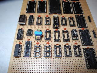
Features
The TS2 computer described in
Microprocessor Systems Design 68000 Hardware, Software, and Interfacing is a single board computer that is capable of operating on its own (with an external serial terminal). It has the following major features:
- 8 MHz 68000 microprocessor.
- Power on and pushbutton reset. LED indicating halt or reset condition.
- Uses commonly available TTL chips for glue logic (no programmable PALs, GALs, FPGAs, etc.)
- 32 KB of static RAM.
- 32 KB of EPROM.
- Full address decoding for peripherals.
- Switches and circuitry for single stepping one instruction at a time.
- Two serial ports to support a terminal and modem/host computer.
- Interrupt encoding and acknowledge circuitry for 8 levels of interrupts.
- Buffered signals running to a backplane connector for expansion.
- On board monitor software that supports downloading, running, and debugging programs.
- All circuitry on a single board (extended double Eurocard 233.4mm x 220mm/9.2in x 8.7in).
CAD Software
The goal of phase 1 of the project was to create a stable schematic, hopefully free of errors. The schematics in the book were almost complete, but omitted some details like bypass capacitors and it was not always clear what gates were parts of the same package. Some circuitry was duplicated across pages to make it clearer to understand.
I decided to enter a schematic into a modern CAD program so I could review it, print it out, and hopefully take advantage of some design rules checking to identify errors like unconnected signals.
For CAD software I ended up using
KiCad, a cross platform and Open Source electronics design automation suite. Some of my requirements were that it would be free, run on Linux, and support basic schematic capture. Overall I found it quite usable. It has a number of quirks, but in my experience all CAD software has usability issues and quite a learning curve and you just have to get used to it. A side benefit was I learned a lot about KiCad, a skill I can reuse on other projects.
Schematic Entry
Entering the schematic, I mostly followed the pages that were in the text book. There were some minor errors and unknowns to figure out. Because many signals get buffered, it was not always clear if signals like AS* were the raw ones on the CPU or the versions coming from buffers. I tried to figure this out as well as possible. I may find errors when I get to testing it.
There were a few errors in pin numbers and some chips were not marked for their type, but I was able to puzzle it out. Since I made some changes to the design, my design is a little different in terms of the parts and their identifiers.
The values of pullup resistors were not all listed. 4.7K seems to be suitable (and is what the Motorola ECB used) so I used this value everywhere.
Some parts are duplicated across pages in the book (like the RESET LED, for example), which helped readers of the book but needed to be corrected in the CAD schematic.
I almost overlooked the fact that there are actually 4 RAM chips and 4 ROM chips! The text shows the circuitry for half of the RAM and ROM, and only in the text does it mention that the circuit is duplicated again using other chip selects.
The original circuit used an 8 MHz clock but provided a divider so the board could run at slower speeds (e.g. 4, 2, 1 MHz) if desired. I didn't see a good reason not to run it at 8 MHz once it got past the breadboard stage. If needed I might plug in a 1 MHz clock oscillator chip in place of 8 MHz for testing purposes.
Circuit Changes
I made a number of changes to simply it and remove features I did not expect to use.
I plan to use EEPROM chips (which are electrically eraseable) rather than EPROMs, which need to be erased under ultravilet light. This will save time when reprogramming them. They are pin compatible with the 2764 EPROMs in the original design.
I didn't implement backplane signals and associated buffering, as I don't expect to expand the board with peripheral cards.
Without any peripherals, there is no need for interrupt encoding and acknowledge circuitry. This could always be added later if needed. One could run two IRQ signals to the two 6850 UARTs, but the monitor software as written does not use interrupts.
I simplified the RS-232 interface, omitting the line drivers and receivers since I plan to directly connect the 6850 UARTs to TTL level FTDI USB to serial convertors. This also allowed removing the requirement for +12 and -12 volt power supplies. I also omitted the strange circuit that can mirror one serial port to the other in a transparent mode as I don't see a need for it.
Design Files
The schematic entry took a while, mostly because I was using KiCad for the first time. I was able to use its rule checker to catch a lot of errors.
The current files are
on github here, which also includes the software as it develops. The KiCad files
are here where
v1 is the original circuit from the book (possibly with some errors) and
v2 is the modified design that I am building.
If you don't have KiCad, there is a
PDF version of the schematic there but it may not always be entirely up to date as it needs to be manually generated from the design files.
For anyone interested, keep in mind that the circuit (as of this writing) has never been built and tested yet. I will update the design as the project progresses.


